
FMUSER RF Power Amplifier Voltage Test Bench for AM Transmitter Power Amplifier (PA) and Buffer Amplifier Testing
FEATURES
- Price (USD): Contact for more
- Qty (PCS): 1
- Shipping (USD): Contact for more
- Total (USD): Contact for more
- Shipping Method: DHL, FedEx, UPS, EMS, By Sea, By Air
- Payment: TT(Bank Transfer), Western Union, Paypal, Payoneer
RF Power Amplifier Board Testing | AM Commissioning Solution from FMUSER
RF power amplifiers and buffer amplifiers are the most important parts of AM transmitters and always play a key role in early design, delivery, and post-maintenance.
These basic components enable the correct transmission of RF signals. Depending on the power level and the strength required by the receiver to identify and decode the signal, any damage can leave broadcast transmitters with signal distortion, reduced power consumption, and more.

For the later overhaul and maintenance of the core components of broadcast transmitters, some important testing equipment is essential. FMUSER's RF measurement solution helps you to verify your design through unparalleled RF measurement performance.
How it Works
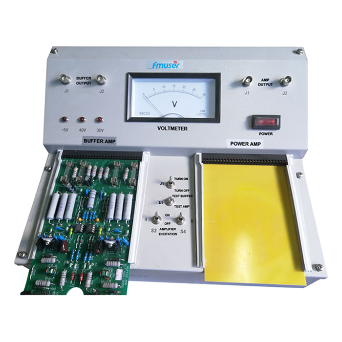
It is mainly used for testing when the power amplifier board and buffer amplifier board of the AM transmitter cannot be confirmed after repair.
Features
- The power supply of the test bench is AC220V, and the panel has a power switch. Internally generated -5v, 40v, and 30v are provided by the built-in switching power supply.
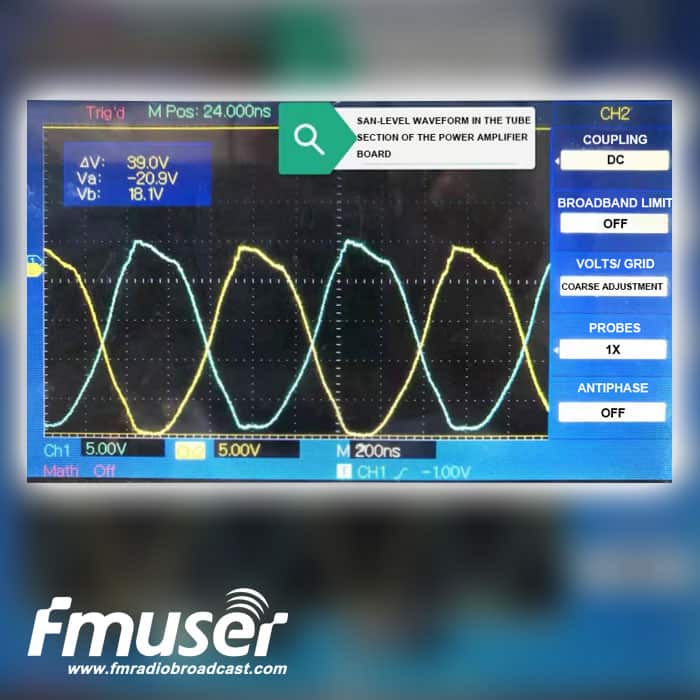
- There are buffer output test Q9 interfaces on the upper part of the test bench: J1 and J2, power amplifier output test Q9 interfaces: J1 and J2, and power amplifier voltage indicator (59C23). J1 and J2 are connected to the double-integrated oscilloscope.
- The left side of the lower part of the test bench is the buffer amplification test position, and the right side is the power amplifier board test.
Instructions
- J1: Test the power switch
- S1: Amplifier board test and buffer board test selector switch
- S3/S4: Power amplifier board test left and right turn-on signal turn-on or turn-off selection.
RF Power Amplifier: What it is and How it Works?
In the radio field, an RF power amplifier (RF PA), or radio frequency power amplifier is a common electronic device used to amplify and output input content, which is often expressed as voltage or power, while the RF power amplifier's function is to raise the things it "absorbs" to a certain level and "export it to the outside world."
How does it Work?
Usually, the RF power amplifier is built into the transmitter in the form of a circuit board. Of course, the RF power amplifier can also be a separate device connected to the output of the low-power output transmitter through a coaxial cable. Due to the limited space, if you are interested, welcome Leave a comment and I'll update it someday in the future :).
The significance of the RF power amplifier is to obtain a sufficiently large RF output power. This is because, first of all, in the front-end circuit of the transmitter, after the audio signal is input from the audio source device through the data line, it will be converted into a very weak RF signal through modulation, but these weak signals are not enough to meet the large-scale broadcast coverage. Therefore, these RF modulated signals go through a series of amplification (buffer stage, intermediate amplification stage, final power amplification stage) through the RF power amplifier until it is amplified to sufficient power and then passed through the matching network. Finally, it can be fed to the antenna and radiated out.
For receiver operation, the transceiver or transmitter-receiver unit can have an internal or external transmit/receive (T/R) switch. The job of the T/R switch is to switch the antenna to the transmitter or receiver as needed.
What is the Basic Structure of an RF Power Amplifier?
The main technical indicators of RF power amplifiers are output power and efficiency. How to improve output power and efficiency is the core of the design goals of RF power amplifiers.
The RF power amplifier has a specified operating frequency, and the selected operating frequency must be within its frequency range. For an operating frequency of 150 megahertz (MHz), an RF power amplifier in the range of 145 to 155 MHz would be suitable. An RF power amplifier with a frequency range of 165 to 175 MHz will not be able to operate at 150 MHz.
Usually, in the RF power amplifier, the fundamental frequency or a certain harmonic can be selected by the LC resonant circuit to achieve distortion-free amplification. In addition to this, the harmonic components in the output should be as small as possible to avoid interference with other channels.
RF power amplifier circuits may use transistors or integrated circuits to generate amplification. In RF power amplifier design, the goal is to have sufficient amplification to produce the desired output power, while allowing for a temporary and small mismatch between the transmitter and antenna feeder and the antenna itself. The impedance of the antenna feeder and the antenna itself is usually 50 ohms.
Ideally, the antenna and feed line combination will present a purely resistive impedance at the operating frequency.
Why RF Power Amplifier is Necessary?
As the main part of the transmitting system, the importance of the RF power amplifier is self-evident. We all know that a professional broadcast transmitter often includes the following parts:
- Rigid shell: usually made of aluminum alloy, the higher the price.
- Audio input board: mainly used to obtain signal input from the audio source, and connect the transmitter and the audio source by an audio cable (such as XLR, 3.45MM, etc.). The audio input board is usually placed on the back panel of the transmitter and is a rectangular parallelepiped with an aspect ratio of approximately 4:1.
- Power supply: It is used for power supply. Different countries have different power supply standards, such as 110V, 220V, etc. In some large-scale radio stations, the common power supply is a 3 Phase 4 Wire System (380V/50Hz) according to the standard. It is also an industrial land according to the standard, which is different from the civil electricity standard.
- Control panel and modulator: usually located in the most conspicuous position on the front panel of the transmitter, composed of the installation panel and some function keys (knob, control keys, display screen, etc.), mainly used to convert the audio input signal into RF signal (very faint).
- RF power amplifier: usually refers to the power amplifier board, which is mainly used to amplify the weak RF signal input from the modulation part. It consists of a PCB and a series of complex component etchings (such as RF input lines, power amplifier chips, filters, etc.), and It is connected to the antenna feeder system through the RF output interface.
- Power supply and fan: The specifications are made by the transmitter manufacturer, mainly used for power supply and heat dissipation
Among them, the RF power amplifier is the most core, the most expensive, and the most easily burned part of the transmitter, which is mainly determined by how it works: the output of the RF power amplifier is then connected to an external antenna.
Most antennas can be tuned so that when combined with the feeder, they provide the most ideal impedance for the transmitter. This impedance matching is required for maximum power transfer from the transmitter to the antenna. Antennas have slightly different characteristics in the frequency range. An important test is to ensure that the reflected energy from the antenna to the feeder and back to the transmitter is low enough. When the impedance mismatch is too high, the RF energy sent to the antenna can return to the transmitter, creating a high standing wave ratio (SWR), causing the transmit power to stay in the RF power amplifier, causing overheating and even damage to active components.
If the amplifier can have good performance, then it can contribute more, which reflects its own "value", but if there are certain problems with the amplifier, then after starting to work or working for a period of time, not only can it no longer Provide any "contribution", but there may be some unexpected "shocks". Such "shocks" are disastrous for the outside world or the amplifier itself.
Buffer amplifier: What it is and How it Works?
Buffer amplifiers are used in AM transmitters.
The AM transmitter consists of an oscillator stage, a buffer and multiplier stage, a driver stage, and a modulator stage, where the main oscillator powers the buffer amplifier, followed by the buffer stage.
The stage next to the oscillator is called a buffer or buffer amplifier (sometimes simply called a buffer) - so named because it isolates the oscillator from the power amplifier.
According to Wikipedia, a buffer amplifier is an amplifier that provides electrical impedance conversion from one circuit to another in order to protect the signal source from any current (or voltage, for a current buffer) that the load may produce.
In fact, on the transmitter side, the buffer amplifier is used to isolate the main oscillator from the other stages of the transmitter, without the buffer, once the power amplifier changes, it will reflect back to the oscillator and cause it to change frequency, and if the oscillation If the transmitter changes the frequency, the receiver will lose contact with the transmitter and receive incomplete information.
How does it Work?
The main oscillator in an AM transmitter produces a stable sub-harmonic carrier frequency. The crystal oscillator is used to generate this stable sub-harmonic oscillation. After that, the frequency is increased to the desired value by means of a harmonic generator. The carrier frequency should be very stable. Any change in this frequency can cause interference to other transmitting stations. As a result, the receiver will accept programs from multiple transmitters.
Tuned amplifiers that provide high input impedance at the main oscillator frequency are buffer amplifiers. It helps prevent any change in load current. Due to its high input impedance at the operating frequency of the main oscillator, changes do not affect the main oscillator. Therefore, the buffer amplifier isolates the main oscillator from the other stages so that loading effects do not change the frequency of the main oscillator.
RF Power Amplifier Test Bench: What it is and How it Works
The term "test bench" uses a hardware description language in digital design to describe the test code that instantiates the DUT and runs the tests.
Test Bench
A test bench or test workbench is an environment used to verify the correctness or sanity of a design or model.
The term originated in the testing of electronic equipment, where an engineer would sit on a lab bench, hold measurement and manipulation tools such as oscilloscopes, multimeters, soldering irons, wire cutters, etc., and manually verify the correctness of the device under test (DUT).
In the context of software or firmware or hardware engineering, a test bench is an environment in which a product under development is tested with the help of software and hardware tools. In some cases, the software may require minor modifications to work with the testbench, but careful coding ensures that changes can be easily undone and no bugs are introduced.
Another meaning of "test bed" is an isolated, controlled environment, very similar to a production environment, but neither hide nor visible to the public, customers, etc. It is therefore safe to make changes as no end user is involved.
RF Device under Test (DUT)
A device under test (DUT) is a device that has been tested to determine performance and proficiency. A DUT can also be a component of a larger module or unit called a unit under test (UUT). Check the DUT for defects to ensure the device is working properly. The test is designed to prevent damaged devices from reaching the market, which can also reduce manufacturing costs.
A device under test (DUT), also known as a device under test (EUT) and a unit under test (UUT), is a manufactured product inspection that is tested when first manufactured or later in its life cycle as part of ongoing functional testing and calibration. This can include post-repair testing to determine whether the product performs to the original product specifications.
In semiconductor tests, the device under test is a die on a wafer or the final packaged part. Using the connection system, connect components to automatic or manual test equipment. The test equipment then powers the component, provides stimulus signals, and measures and evaluates the output of the equipment. In this way, the tester determines whether the particular device under test meets the device specification.
In general, an RF DUT can be a circuit design with any combination and number of analog and RF components, transistors, resistors, capacitors, etc., suitable for simulation with the Agilent Circuit Envelope Simulator. More complex RF circuits will take more time to simulate and consume more memory.
Testbench simulation time and memory requirements can be thought of as a combination of benchmark testbench measurements with the requirements of the simplest RF circuit plus the circuit envelope simulation requirements of the RF DUT of interest.
An RF DUT connected to a wireless test bench can often be used with the test bench to perform default measurements by setting the test bench parameters. Default measurement parameter settings are available for a typical RF DUT:
- An input (RF) signal with a constant radio frequency carrier frequency is required. The output of the test bench RF signal source does not produce an RF signal whose RF carrier frequency varies with time. However, the test bench will support an output signal containing RF carrier phase and frequency modulation, which can be represented by appropriate I and Q envelope changes at a constant RF carrier frequency.
- An output signal with a constant RF carrier frequency is produced. The test bench input signal must not contain a carrier frequency whose frequency varies over time. However, the test bench will support input signals that contain RF carrier phase noise or the time-varying Doppler shift of the RF carrier. These signal perturbations are expected to be represented by suitable I and Q envelope changes at a constant RF carrier frequency.
- An input signal from a signal generator with 50-ohm source resistance is required.
- An input signal without spectral mirroring is required.
- Generate an output signal that requires an external load resistor of 50 ohms.
- Produces an output signal without spectral mirroring.
- Rely on the test bench to perform any measurement-related bandpass signal filtering of the RF DUT output signal.
AM Transmitter Basics You Should Know
A transmitter that emits an AM signal is called an AM transmitter. These transmitters are used in the medium wave (MW) and short wave (SW) frequency bands of AM broadcasting. The MW band has frequencies between 550 kHz and 1650 kHz and the SW band has frequencies from 3 MHz to 30 MHz.
The two types of AM transmitters used based on transmit power are:
- high level
- low level
High-level transmitters use high-level modulation, and low-level transmitters use low-level modulation. The choice between the two modulation schemes depends on the transmit power of the AM transmitter. In broadcast transmitters whose transmit power may be on the order of kilowatts, high-level modulation is used. In low-power transmitters that only require a few watts of transmit power, low-level modulation is used.
High and low-level transmitters
The figure below shows the block diagram of the high-level and low-level transmitters. The basic difference between the two transmitters is the power amplification of the carrier and modulated signals.
Figure (a) shows a block diagram of an advanced AM transmitter.
Figure (a) is drawn for audio transmission. In high-level transmission, the power of the carrier and modulated signals is amplified before being applied to the modulator stage, as shown in Figure (a). In low-level modulation, the power of the two input signals to the modulator stage is not amplified. The required transmit power is obtained from the last stage of the transmitter, the Class C power amplifier.
The parts of Figure (a) are:
- Carrier Oscillator
- Buffer Amplifier
- Frequency Multiplier
- Power Amplifier
- Audio Chain
- Modulated Class C Power Amplifier
- Carrier Oscillator
A carrier oscillator generates a carrier signal in the radio frequency range. The frequency of the carrier is always high. Since it is difficult to generate high frequencies with good frequency stability, carrier oscillators generate submultiples with the desired carrier frequency. This sub-octave is multiplied by the multiplier stage to obtain the desired carrier frequency. Also, a crystal oscillator can be used at this stage to generate a low-frequency carrier with the best frequency stability. The frequency multiplier stage then increases the carrier frequency to its desired value.
Buffer Amp
The purpose of the buffer amplifier is twofold. It first matches the output impedance of the carrier oscillator with the input impedance of the frequency multiplier, the next stage of the carrier oscillator. It then isolates the carrier oscillator and frequency multiplier.
This is necessary so that the multiplier does not draw large currents from the carrier oscillator. If this happens, the frequency of the carrier oscillator will not be stable.
Frequency Multiplier
The sub-multiplied frequency of the carrier signal produced by the carrier oscillator is now applied to the frequency multiplier through the buffer amplifier. This stage is also known as a harmonic generator. The frequency multiplier produces higher harmonics of the carrier oscillator frequency. A frequency multiplier is a tuned circuit that tunes to the carrier frequency that needs to be transmitted.
Power Amp
The power of the carrier signal is then amplified in a power amplifier stage. This is a basic requirement for a high-level transmitter. Class C power amplifiers provide high-power current pulses of the carrier signal at their outputs.
Audio Chain
The audio signal to be transmitted is obtained from the microphone as shown in Figure (a). The audio driver amplifier amplifies the voltage of this signal. This amplification is necessary to drive audio power amplifiers. Next, a Class A or Class B power amplifier amplifies the power of the audio signal.
Modulated Class C Amplifier
This is the output stage of the transmitter. The modulated audio signal and carrier signal is applied to this modulation stage after power amplification. The modulation occurs at this stage. The Class C amplifier also amplifies the power of the AM signal to the regained transmit power. This signal is ultimately passed to the antenna, which radiates the signal into the transmission space.
Figure (b): Low-Level AM Transmitter Block Diagram
The low-level AM transmitter shown in Figure (b) is similar to the high-level transmitter except that the power of the carrier and audio signals is not amplified. These two signals are applied directly to the modulated Class C power amplifier.
The modulation occurs during this phase, and the power of the modulated signal is amplified to the desired transmit power level. The transmitting antenna then transmits the signal.
Coupling of output stage and antenna
The output stage of the modulated class C power amplifier feeds the signal to the transmit antenna. To transfer maximum power from the output stage to the antenna, the impedances of the two sections must match. For this, a matching network is required. The match between the two should be perfect at all transmit frequencies. Since matching at different frequencies is required, inductors and capacitors that provide different impedances at different frequencies are used in the matching network.
A matching network must be constructed using these passive components. As shown in Figure (c) below.
Figure (c): Dual Pi matching network
The matching network used to couple the transmitter output stage and the antenna is called a dual π network. The network is shown in Figure (c). It consists of two inductors L1 and L2 and two capacitors C1 and C2. The values of these components are chosen so that the input impedance of the network is between 1 and 1'. Figure (c) is shown to match the output impedance of the transmitter output stage. Furthermore, the output impedance of the network matches the impedance of the antenna.
The double π matching network also filters out unwanted frequency components that appear at the output of the last stage of the transmitter. The output of a modulated Class C power amplifier may contain highly undesirable higher harmonics, such as second and third harmonics. The frequency response of the matching network is set to completely reject these unwanted higher harmonics and only the desired signal is coupled to the antenna.
CONTACT US


FMUSER INTERNATIONAL GROUP LIMITED.
We are always providing our customers with reliable products and considerate services.
If you would like to keep touch with us directly, please go to contact us
-
![Home]()
Home
-
![Tel]()
Tel
-
![Email]()
Email
-
![Contact]()
Contact


